AI Term of the Moment
Native Processing Unit
Redirected from: chip creation
Definition: chip manufacturing
The making of an integrated circuit (IC), commonly known as a "chip." For a list of chip companies in this encyclopedia, see semiconductor companies.
Quite Incredible
The chip is the most amazing product humans have ever conceived. The actual working area of the state-of-the-art chips that power the latest phones and computers is a sliver of silicon about the size of a postage stamp, only 700 times thinner. It contains billions of transistors that function as on/off switches. The transistor is the chip's fundamental component. See transistor.
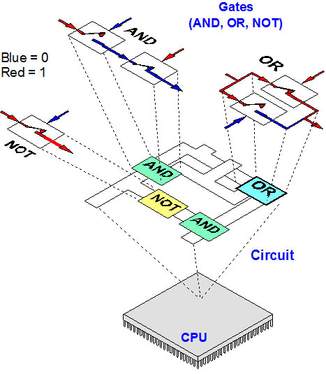
Transistors to Gates to Circuits

FROM LOGIC TO PLUMBING
Circuits were originally designed by humans. Today, logic functions reside in digital libraries, and designers pick and choose from a menu. However, new circuits have to be designed by humans, gate by gate.


Inspecting the Plumbing
CHIPS ARE JUST ROCKS
The base material of a chip is usually silicon, although materials such as sapphire and gallium arsenide are also used. Found in quartz rocks, the silicon is purified in a molten state and then chemically combined (doped) with other materials to alter its electrical properties. The result is a silicon crystal ingot that is either positively (p-type) or negatively charged (n-type). Slices of the ingot approximately 1/30th of an inch thick are cut from this "crystal salami" that is 3.9" to 17.7" in diameter to become "wafers," which is the starting point of chip making.


Drawing the Ingot
BUILDING THE LAYERS
Circuit building starts out by adhering a layer of silicon dioxide insulation on the wafer's surface. The insulation is coated with film and exposed to ultraviolet light through the first photomask, hardening the film and insulation below it. The unhardened areas are etched away exposing the silicon base below. By shooting a gas under heat and pressure into the exposed silicon (diffusion), a sublayer with different electrical properties is created beneath the surface.

Mask, Etch, Diffuse

Inspecting Wafers

Testing Wafers

Packaging the Chip
The Future
There is a never-ending thirst to build more and more transistors onto a single chip. In the early 1980s, the IBM PC's 8088 CPU had 25 thousand. In the 2020s, chips have tens of billions of transistors for computers and smartphones. See chip feature size and Versal.
From a CPU to an Entire System
Just as the chip eliminated cutting apart the transistors only to be reconnected in patterns, increasingly, more functions are built onto the same chip, creating a complete system-on-chip (see SoC).
It's Science Fiction - Wrap Your Mind Around This
A single chip with an active transistor area the size of a postage stamp, only much thinner, can contain more than 50 billion interconnected transistors in multiple layers. That equates to more than 100 million transistors per square millimeter, or about the same space as the head of a pin. See active area.
Building the Transistor
Although the following illustrations show one transistor, many transistors go through these stages at the same time. The following diagrams are conceptual because today's chips are way more complex.


The FinFET Transistor

Dressing for Work


No Germs in these Rooms

The World Depends on Chips

Quite Incredible
The chip is the most amazing product humans have ever conceived. The actual working area of the state-of-the-art chips that power the latest phones and computers is a sliver of silicon about the size of a postage stamp, only 700 times thinner. It contains billions of transistors that function as on/off switches. The transistor is the chip's fundamental component. See transistor.
Pulses cause transistors to open or close, and the current flowing through one affects the opening or closing of another and so on. Transistors are wired together in Boolean logic gates. Gates make up circuits, and circuits make up CPUs, GPUs and microcontrollers. For simplification in this example, the gates are illustrated as mechanical switches. See transistor, Boolean Logic, CPU, GPU and microcontroller.
FROM LOGIC TO PLUMBING
Circuits were originally designed by humans. Today, logic functions reside in digital libraries, and designers pick and choose from a menu. However, new circuits have to be designed by humans, gate by gate.
People are always more flexible than computers and can find flaws that might go undetected by software analysis. (Image courtesy of Elxsi Corporation.)
CHIPS ARE JUST ROCKS
The base material of a chip is usually silicon, although materials such as sapphire and gallium arsenide are also used. Found in quartz rocks, the silicon is purified in a molten state and then chemically combined (doped) with other materials to alter its electrical properties. The result is a silicon crystal ingot that is either positively (p-type) or negatively charged (n-type). Slices of the ingot approximately 1/30th of an inch thick are cut from this "crystal salami" that is 3.9" to 17.7" in diameter to become "wafers," which is the starting point of chip making.
The silicon ingot is being drawn from a scalding furnace containing molten silicon. High-speed saws slice the ingot into wafers about as thick as a dime, which will then be ground thinner and polished like a mirror. (Image courtesy of Texas Instruments, Inc.)
BUILDING THE LAYERS
Circuit building starts out by adhering a layer of silicon dioxide insulation on the wafer's surface. The insulation is coated with film and exposed to ultraviolet light through the first photomask, hardening the film and insulation below it. The unhardened areas are etched away exposing the silicon base below. By shooting a gas under heat and pressure into the exposed silicon (diffusion), a sublayer with different electrical properties is created beneath the surface.
Through multiple stages of masking, which creates a pattern, etching, which opens up an area, and diffusion, which alters the silicon properties, the chip's sublayers are created. The final stage lays the top metal layers (usually aluminum) that interconnect the transistors to each other and to the outside world. For more about the masking stages, see reticle.
The technician is wearing a "bunny suit" but not a mask, because the wafers have already been manufactured. These are six-inch wafers, and although not state-of-the-art, are still widely used. (Image courtesy of Hewlett-Packard Company.)
Bad chips are marked for elimination while the good ones are sliced out, placed into packages and connected by tiny wires or solder balls. The package is then sealed and tested as a complete unit (see chip package).
This machine bonds the chips to the metal structure that will connect to the pins of the chip package and carry the signals to and from the circuit board. (Image courtesy of Texas Instruments, Inc.)
There is a never-ending thirst to build more and more transistors onto a single chip. In the early 1980s, the IBM PC's 8088 CPU had 25 thousand. In the 2020s, chips have tens of billions of transistors for computers and smartphones. See chip feature size and Versal.
From a CPU to an Entire System
Just as the chip eliminated cutting apart the transistors only to be reconnected in patterns, increasingly, more functions are built onto the same chip, creating a complete system-on-chip (see SoC).
It's Science Fiction - Wrap Your Mind Around This
A single chip with an active transistor area the size of a postage stamp, only much thinner, can contain more than 50 billion interconnected transistors in multiple layers. That equates to more than 100 million transistors per square millimeter, or about the same space as the head of a pin. See active area.
Building the Transistor
Although the following illustrations show one transistor, many transistors go through these stages at the same time. The following diagrams are conceptual because today's chips are way more complex.
The previous transistor steps are much more simplified than today's state-of-the-art transistors. Notice the source, gate and drain on the FinFET above. Although most FinFETs have only one or two fins rather than three, their construction is nevertheless extremely complex. Consider that in advanced chips, there can be more than 100 million of these per square millimeter. See FINFET.
Operations are performed in a "clean room," because air particles can mix with the microscopic mixtures and easily render a wafer worthless. Depending on the complexity, more chips can fail than succeed. Putting on the "bunny suit" is an elaborate procedure. (Image courtesy of Intel Corporation.)
You won't catch the flu working in a chip fabrication plant, at least not in the clean room. Bunny suits and clean rooms are required to produce high yields with as few defects as possible. (Images top to bottom courtesy of Texas Instruments, Inc., Motorola, Inc. and Microchip Technology Inc.)
In the 2020s, people are beginning to realize how important the semiconductor industry is to the global economy. Chris Miller's book covers the history of the industry and the issues facing a world where chip manufacturing is dominated by companies outside the U.S.
To explore the variety of topics in this reference, see What's in this encyclopedia.